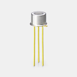
1.Classification according to the manufacturing process used
Operational amplifiers can be divided into two types according to the manufacturing process used: CMOS and bipolar operational amplifiers. Since CMOS operational amplifiers are voltage-controlled devices, they operate with a low DC input bias current (I I), so their power consumption is low. However, due to the low withstand voltage of typical CMOS processes, CMOS operational amplifiers are generally used in applications with a voltage of 5V or lower. In contrast, bipolar processes tolerate higher voltages than CMOS processes. Toshiba’s single-supply and dual-supply bipolar operational amplifiers can be used at supply voltages of 12V and ±18V, respectively.
In addition, bipolar operational amplifiers have an advantage over CMOS operational amplifiers in terms of 1/f noise. The main cause of this noise is the crystal disorder of silicon, which exists in large quantities on the surface of the wafer. Therefore, bipolar transistors whose junction interface is located deep inside the device generate less 1/f noise than MOS transistors whose junction interface is close to the surface of the device. However, in recent years, due to the continuous improvement of CMOS processes, low-noise CMOS operational amplifiers have emerged. Therefore, most applications now use CMOS operational amplifiers.
Bipolar operational amplifiers
2.Classification by power supply type
Operational amplifiers are of two types: single-supply type and dual-supply type. For single-supply operational amplifiers, V CC is positive with respect to GND. For dual-supply operational amplifiers, V CC is positive with respect to GND and V EE is negative with respect to GND. Even single-supply operational amplifiers can use dual supplies as long as the differential input voltage between the minimum and maximum supply voltages does not exceed the differential input voltage range shown in the Absolute Maximum Ratings table. (In this case, attention should be paid to power supply noise because each power supply in the operational amplifier is not referenced to GND.)
However, the power supply voltage range of a typical operational amplifier is usually offset to the GND (negative) side, thereby narrowing the allowable positive power supply voltage range. As an example, some electrical characteristics of the TC75S51FU are shown below. Its common-mode input voltage (CMV IN ) is specified to be 0 to 2.5 V. CMV IN is the allowable input voltage range of the TC75S51FU when it is powered by a single power supply. For example, assume that this operational amplifier is powered by a dual power supply of ±1.5 V. Then, the common-mode input voltage can be restated as -1.5 V to +1.0 V. In this case, when the input voltage is from V CC to 0.5 V, TC75S51FU may not provide normal output, for example, because the gain is reduced.

- Classification by input circuit
The figure below shows the input circuit types of operational amplifiers. The differential input of a typical operational amplifier consists of a pair of P-channel MOSFETs or a pair of N-channel MOSFETs, while the differential input of a rail-to-rail operational amplifier consists of a pair of P-channel MOSFETs and a pair of N-channel MOSFETs. (But in reality, few operational amplifiers have differential inputs consisting of N-channel MOSFETs.) When the input voltage is a few volts lower than V DD, the operational amplifier with P-channel input MOSFET cannot provide normal output. Similarly, when the input voltage is a few volts higher than GND, the operational amplifier with N-channel input MOSFET cannot provide normal output. Rail-to-rail operational amplifiers combine the advantages of these two operational amplifiers and can provide normal output over the entire input range from V DD to GND.

- Classification based on electrical characteristics
In addition to the characteristics described above, op-amps may be classified according to their electrical characteristics. Select op-amps that suit your requirements.
Brand:
Analog Semiconductor is a supplier of analog and mixed-signal chips and solutions. The company was founded in 2018 by a group of local engineers from top international semiconductor companies. The company is headquartered in Shanghai, with R&D and technical support centers in Zhangjiang, Lingang, Suzhou, Shenzhen, Xi’an, and Beijing. The company focuses on chip design in the fields of signal chain, power management, MCU/DSP, and its products are mainly aimed at the industrial, communication, medical, automotive and other markets. Analog’s core mission is to provide customers with high-quality chips and provide the most basic chip support for the world’s technological and intelligent development.
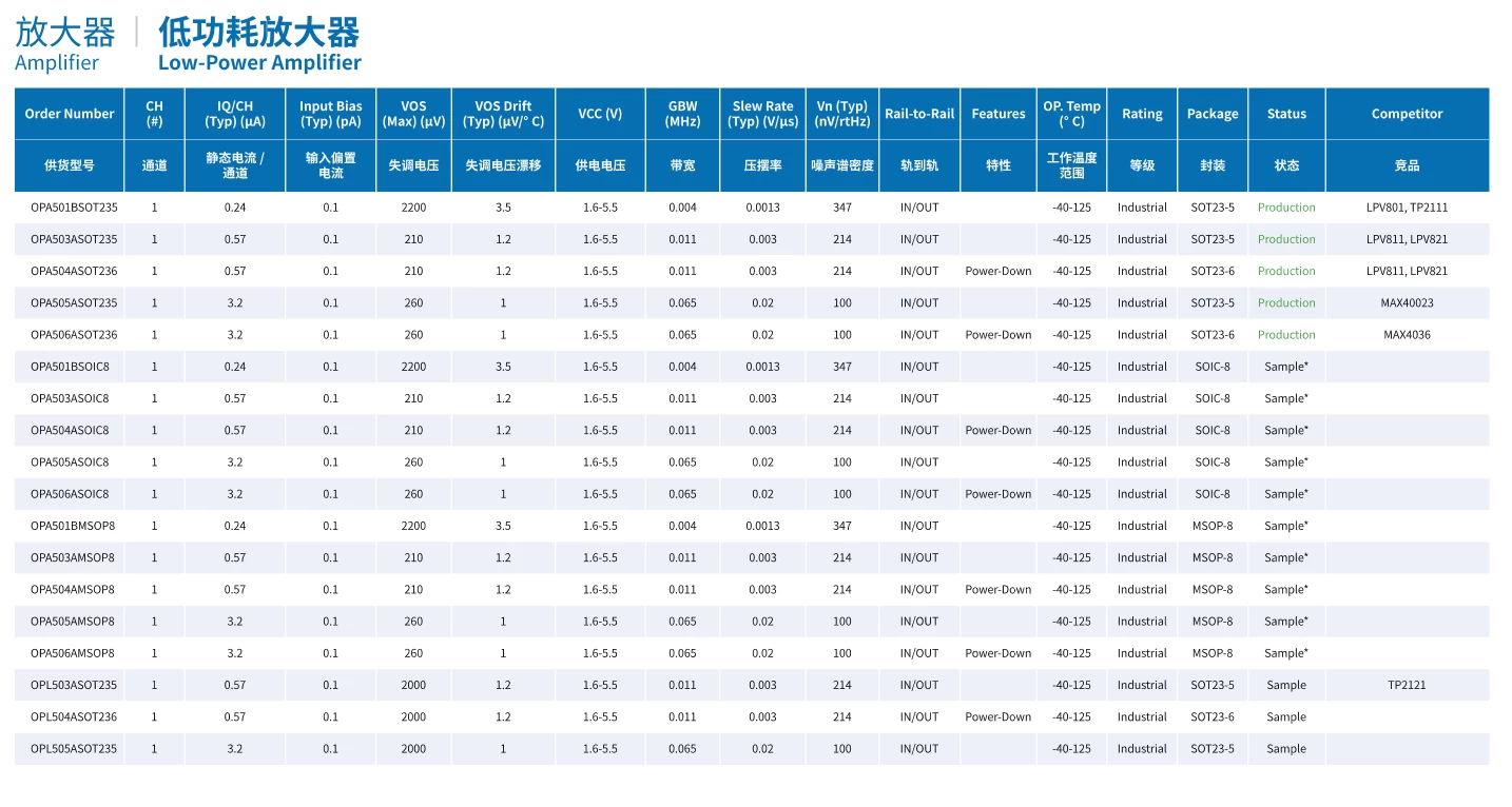
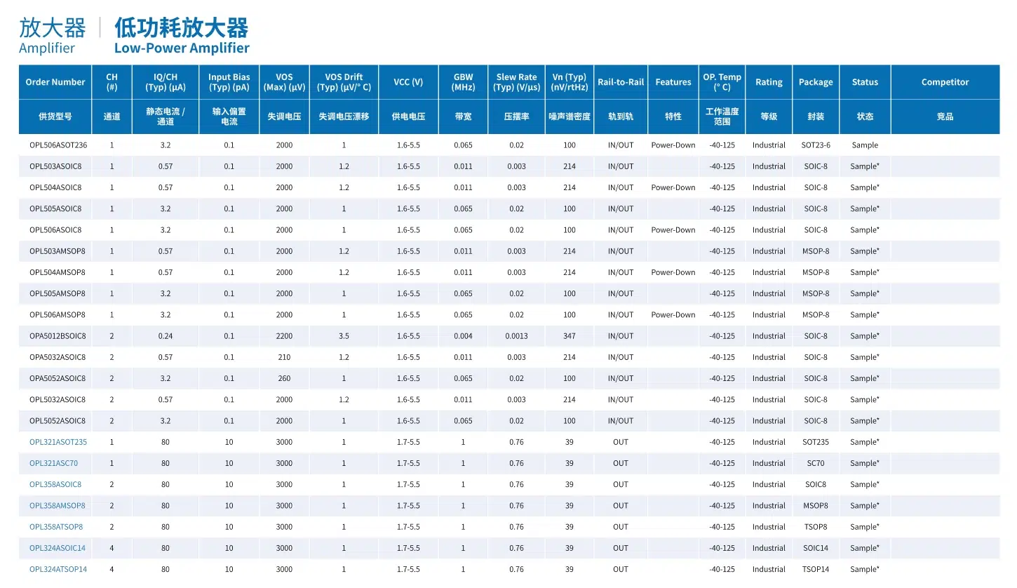
Low Power Amplifier:
Features: Optimized design to reduce power consumption, suitable for battery-powered and power-sensitive applications. Applications: Portable devices, low-power electronic systems, sensor interfaces.

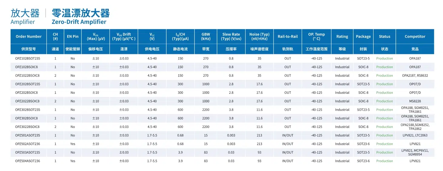
Zero-drift amplifier:
Extremely low temperature drift: Zero-drift operational amplifiers can maintain very stable performance over a wide temperature range, reducing errors caused by temperature changes. High precision: This operational amplifier has low bias current, low bias voltage, and high input impedance, providing high-precision signal processing. Good stability: Even in an environment with large temperature changes, the output signal can be kept consistent, suitable for high-precision measurement and control systems.
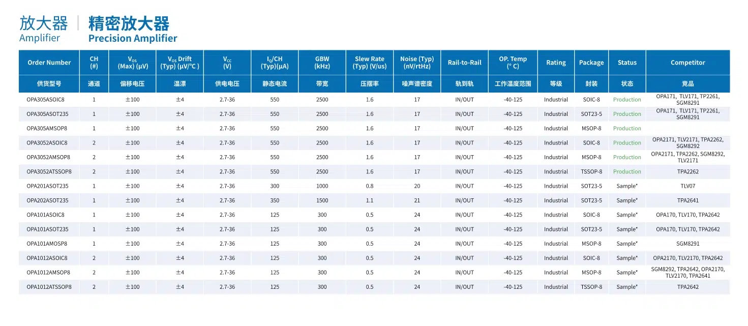
Precision Amplifier:
Features: Very low input bias current, low input deviation voltage, and high input impedance for applications requiring high precision. Applications: Instrumentation amplifier, precision voltage reference, data acquisition.
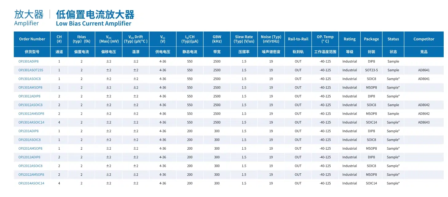
 Low Bias Current Amplifier:
Low Input Bias Current: Has extremely low input bias current, reducing the impact on high impedance circuits, thereby improving signal accuracy. High Input Impedance: Usually has high input impedance to further reduce the loading effect on the signal source. Low Noise: Due to the low input bias current, the noise is also relatively low, which helps to improve the clarity of the signal.
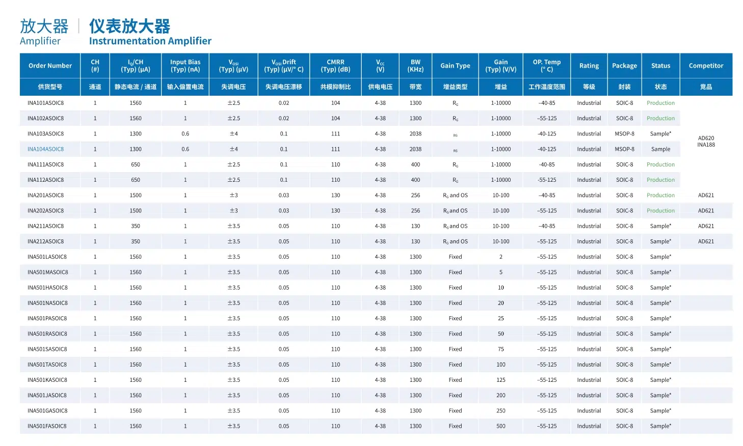
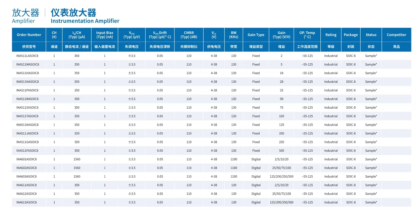
Instrumentation amplifier:
High input impedance: reduces the load effect on the signal source, suitable for applications with high impedance signal sources. High common mode rejection ratio (CMRR): effectively suppresses common mode signals (such as noise or interference) and improves signal accuracy. Low noise: the design focuses on reducing noise to ensure signal clarity and accuracy. Adjustable gain: the gain can usually be adjusted through external resistors to meet different application requirements. High precision: provides stable and accurate signal amplification, suitable for precision measurement and data acquisition.
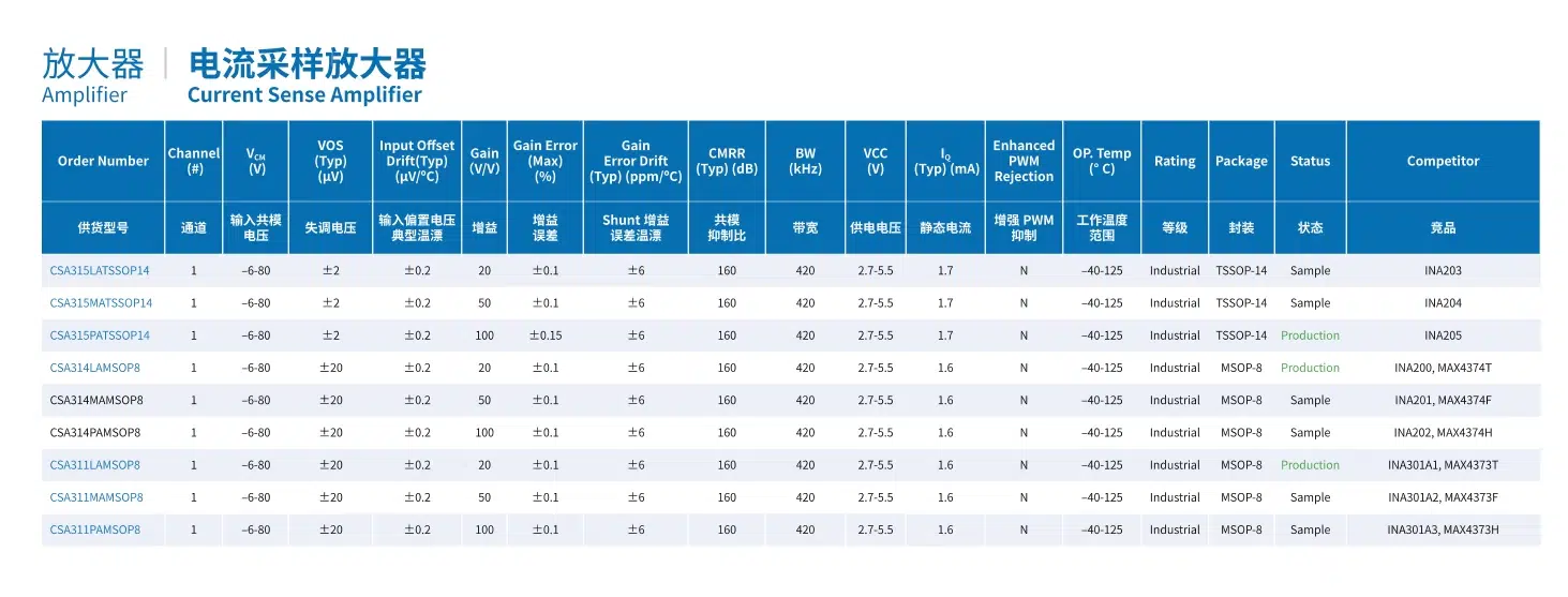
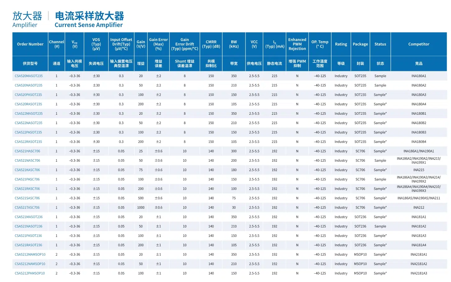
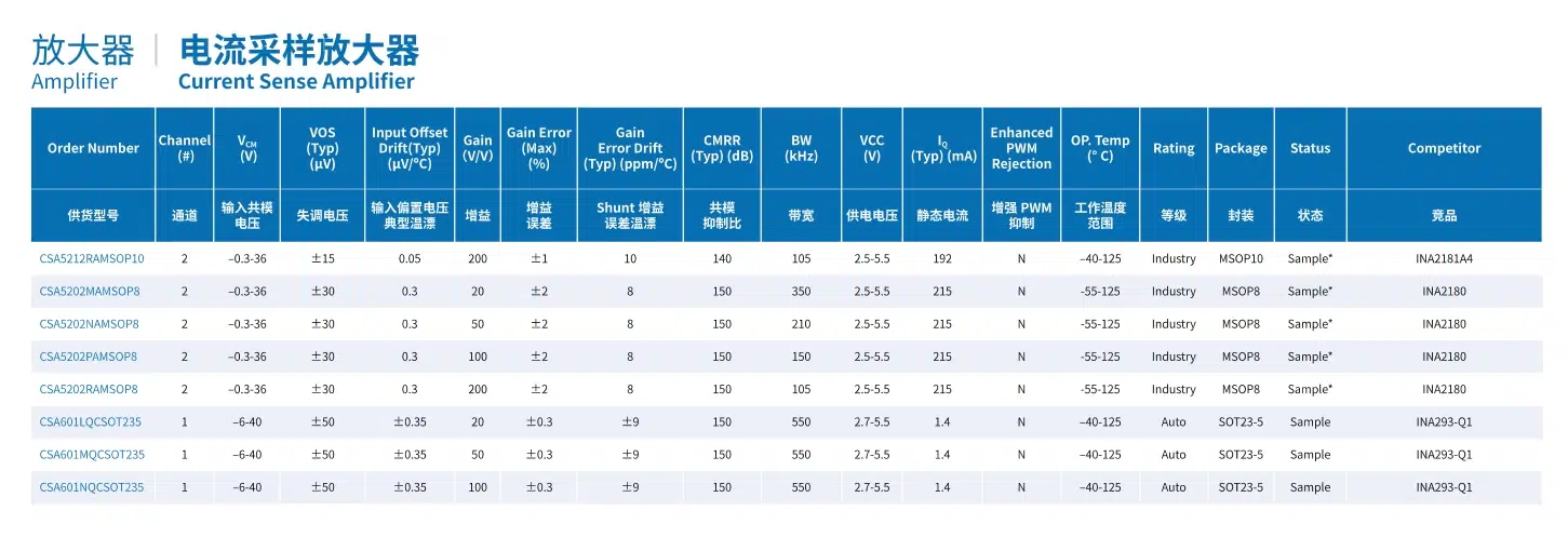
Current Sampling Amplifiers:
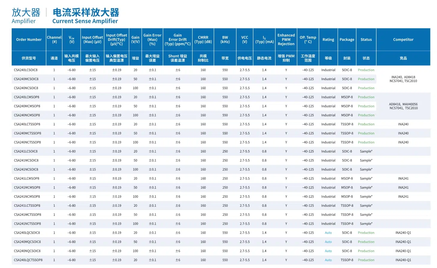
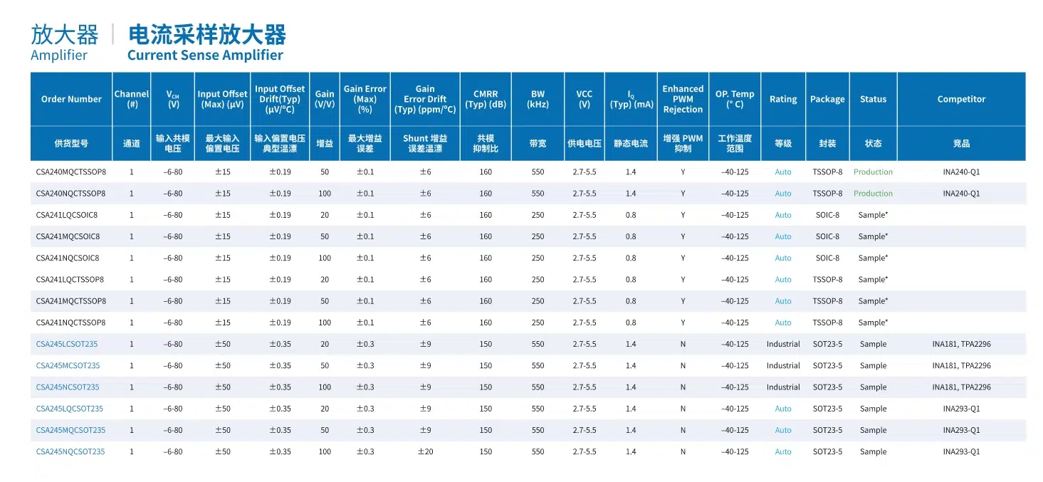
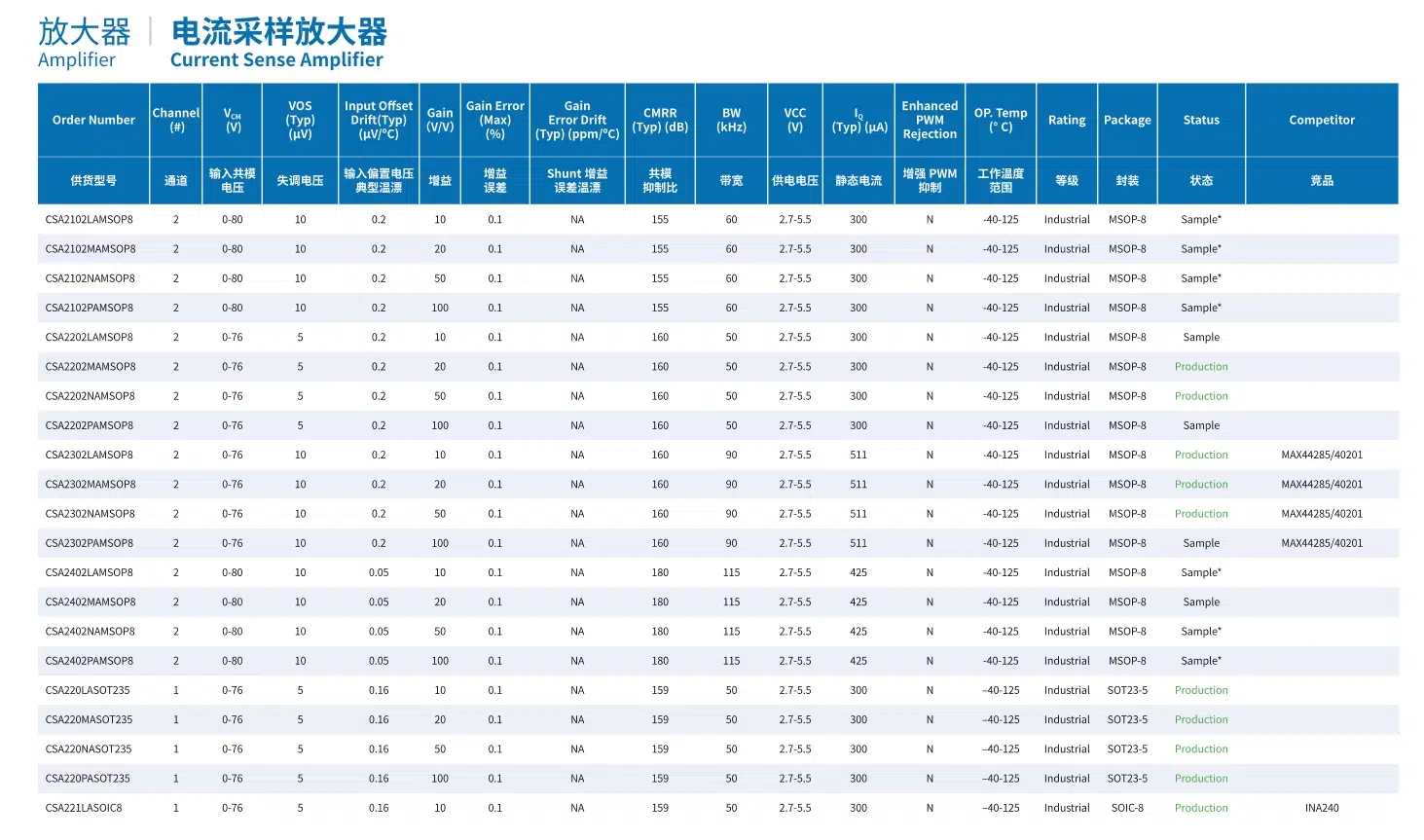
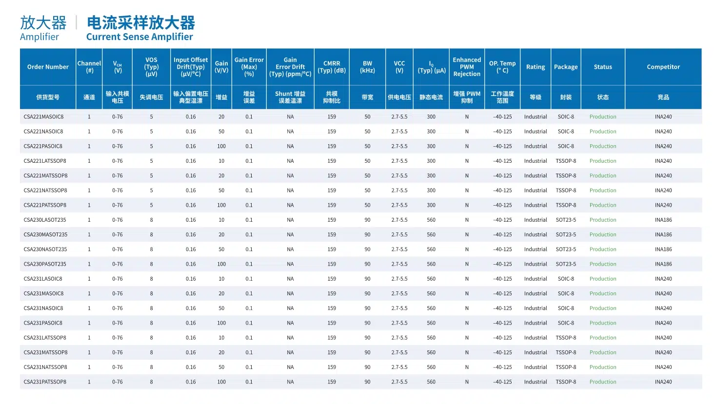
High Common Mode Rejection Ratio (CMRR): Current sampling amplifiers typically have high CMRR to suppress the effects of common mode voltage on current measurement. Low Input Bias Current: Low input bias current reduces measurement errors, especially in high impedance applications. High Gain Accuracy: Provides stable gain to ensure accurate amplification of tiny voltage signals. Low Noise: Designed with a focus on low noise performance to improve measurement accuracy and signal clarity. Wide Bandwidth: Capable of processing signals over a wide frequency range, suitable for fast-changing current measurements.
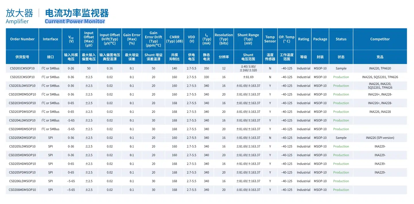
Current Power Monitor:
Special amplifiers:
High gain, low input bias current, low noise. Often used for signal amplification, filtering, and mathematical operations. Provides multiple configurations and application modes, such as inverting amplifier, non-inverting amplifier, integrator, etc.

For more information, please contact us: emi-ic.com


