


In the field of optoelectronics, every precise interaction between light and electricity has the potential to redefine human perception and technological boundaries. As a global leader in this domain, the Japanese brand Hamamatsu continuously pioneers advancements across medical imaging, industrial applications, scientific research, and quantum technologies with its precision optoelectronics, high-performance products, and exceptional “Made in Japan” quality. From detecting microscopic particles to exploring deep space, from breakthroughs in life sciences to the evolution of smart manufacturing, Hamamatsu harnesses the power of light to provide reliable and innovative solutions for customers worldwide.

The Foundation of Light – Hamamatsu’s Core Technology Matrix
At its core, optoelectronic technology revolves around the precise conversion of light into electrical signals or vice versa. With decades of research and development, Hamamatsu has established a comprehensive technological ecosystem covering full-spectrum detection, ultra-high sensitivity, and multi-scenario adaptability, making it a key standard-setter in the industry.
1.1 Revolutionizing High-Sensitivity Detectors: From PMT to SiPM
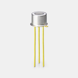
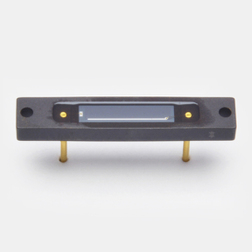
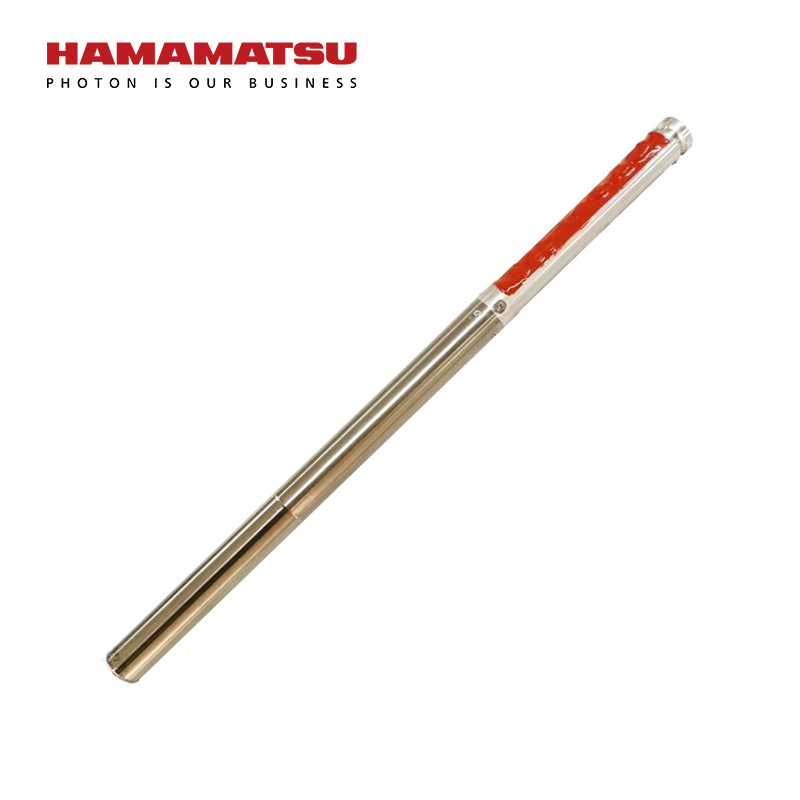
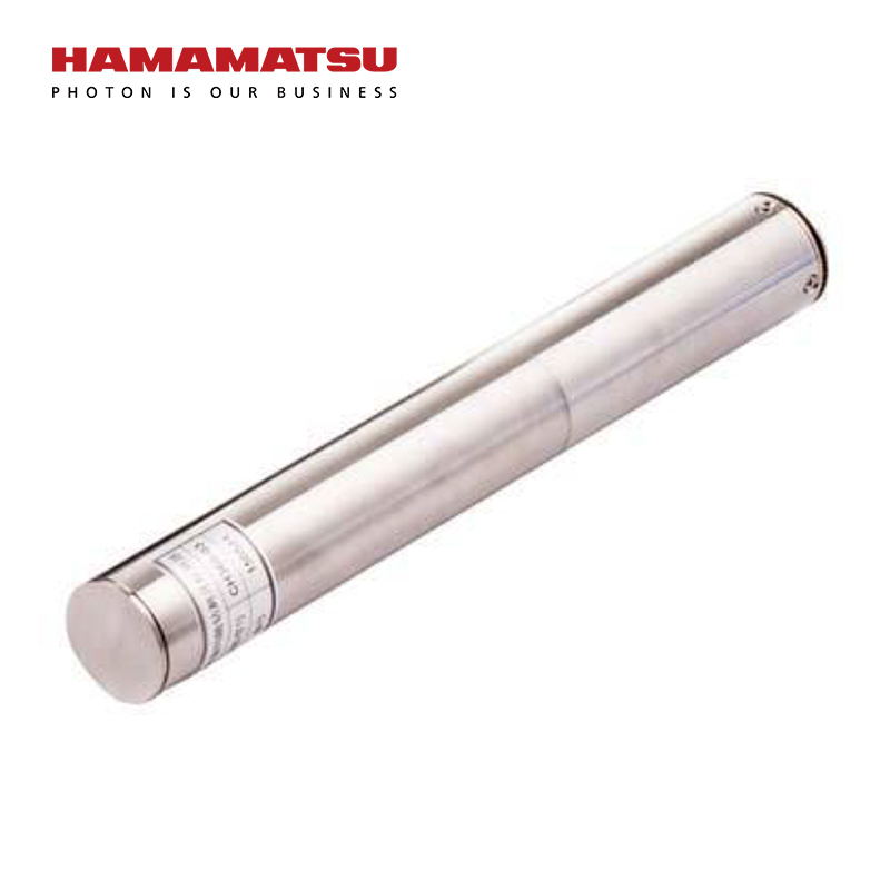
Photomultiplier Tubes (PMT):
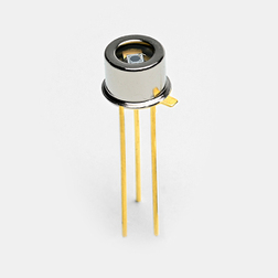
As one of Hamamatsu’s flagship products, photomultiplier tubes (PMTs) utilize an electron multiplication effect within a vacuum tube to achieve single-photon-level high sensitivity. With low noise and a wide dynamic range, PMTs serve as essential sensors in medical imaging (e.g., PET-CT scans) and scientific research (e.g., particle physics experiments).
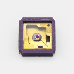
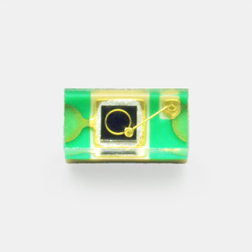
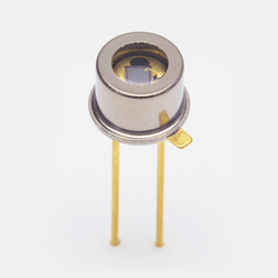
Silicon Photomultipliers (SiPM):
With the advancement of semiconductor technology, Hamamatsu developed SiPM as a solid-state alternative to traditional vacuum tubes, combining the high sensitivity of PMTs with compact size and low power consumption. This innovation has accelerated the development of portable medical devices, automotive sensors (e.g., LiDAR), and quantum technologies (e.g., single-photon detection).
1.2 Full-Spectrum Coverage: Multi-Dimensional Sensing from Infrared to X-rays
Infrared Sensing and UV Detection:
Hamamatsu’s infrared detectors are widely used in environmental monitoring (e.g., greenhouse gas analysis), security systems (e.g., thermal imaging), and life sciences (e.g., DNA sequencing). Meanwhile, its UV sensors play a crucial role in water quality monitoring, flame detection, and precise control in semiconductor lithography.
X-ray Detection:
Hamamatsu’s high-resolution X-ray sensors are critical in medical diagnostics (e.g., digital radiography) and semiconductor inspection. Their multi-layer structure design enables precise defect detection, ensuring strict quality assurance in chip manufacturing.
1.3 Lasers and Image Sensors: The “Optical Arms” of the Smart Era
Lasers:
Hamamatsu’s semiconductor and fiber lasers serve as efficient and stable light sources for industrial processing (e.g., precision cutting), communication systems (e.g., optical modules), and automotive sensors (e.g., autonomous driving LiDAR).
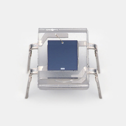
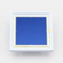
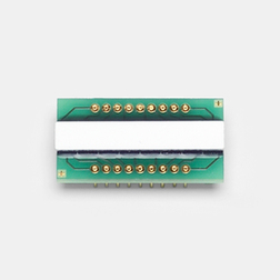
Image Sensors:
From scientific-grade CCDs (used in astronomical observations) to CMOS sensors (used in industrial vision systems), Hamamatsu’s imaging technology delivers ultra-high resolution and low noise, making it the “digital eye” of industrial inspection and scientific research.
The Mission of Light – Hamamatsu’s Technological Contributions Across Industries
Hamamatsu’s impact extends far beyond research labs—it has deeply integrated into society’s critical sectors, becoming the invisible force driving healthcare, industrial progress, and scientific breakthroughs.
2.1 Medical Imaging: The Optoelectronic Power Behind Precision Diagnostics
In early cancer screening, Hamamatsu’s PMTs and SiPMs are core components of PET-CT scanners, capturing the distribution of radioactive tracers inside the body to generate high-contrast tumor images. Additionally, its miniature image sensors in endoscopes and fluorescence detectors in flow cytometry enable cell-level observations, paving the way for advancements in personalized medicine.
2.2 Industrial Inspection: The Gatekeeper of Quality in Smart Manufacturing
Semiconductor Inspection:
As semiconductor fabrication reaches the nanometer scale, Hamamatsu’s X-ray sensors and UV light sources play a crucial role in detecting microscopic defects on wafers, ensuring that each chip meets rigorous reliability standards.
Material Analysis and Non-Destructive Testing:
Infrared thermal imaging and laser scanning systems can non-invasively detect structural abnormalities in materials, making them indispensable in aerospace, renewable energy, and high-end manufacturing.
2.3 Frontier Research: Pioneering Optoelectronic Exploration of the Unknown
Quantum Technology:
Hamamatsu’s ultra-low-noise single-photon detectors are vital for quantum communication (e.g., QKD encryption) and quantum computing experiments, helping researchers develop the next generation of information security systems.
Cosmic Exploration and Fundamental Physics:
From neutrino detection in the Super-Kamiokande Observatory to dark matter research in deep underground laboratories, Hamamatsu’s PMTs play a key role in uncovering the mysteries of the universe.
2.4 Automotive & Consumer Electronics: The Optoelectronic Engine of Smart Technologies
With the rise of autonomous driving, Hamamatsu’s LiDAR lasers and sensors provide real-time 3D environmental mapping for vehicles. Additionally, proximity sensors in smartphones and miniaturized optical modules in AR/VR devices rely on Hamamatsu’s advanced optoelectronic technology.
The Philosophy of Light – The Brand Ethos Behind “Made in Japan”
Hamamatsu’s success is not just built on technological leadership—it is rooted in its core values: precision, innovation, and reliability, as well as the unwavering pursuit of excellence associated with Japanese craftsmanship.
3.1 Innovation-Driven Growth: From Research to Market Deployment
Hamamatsu reinvests approximately 10% of its revenue into R&D annually, establishing a full research-to-product pipeline. For instance, its SiPM technology transitioned from concept to mass production within five years, rapidly capturing emerging markets.
3.2 The “Zero-Defect” Promise of Japanese Manufacturing
From material selection to ultra-cleanroom production, Hamamatsu adheres to a strict zero-defect philosophy. Every product undergoes hundreds of reliability tests, including extreme temperature, vibration, and long-term aging assessments, ensuring flawless performance in critical applications like medical and aerospace technologies.
3.3 Global Collaboration & Localized Service
While maintaining its core “Made in Japan” production, Hamamatsu operates over 20 technical centers and offices worldwide, offering customized solutions. Examples include radiation-resistant detectors for CERN and high-speed inspection modules for Asian semiconductor manufacturers.
The Future of Light – Hamamatsu’s Next-Generation Vision
As the world moves toward artificial intelligence, quantum computing, and carbon neutrality, Hamamatsu is positioning its optoelectronic expertise at the forefront of three strategic directions:
- Miniaturization & Integration: Developing smaller, lower-power sensors for wearable devices and IoT applications.
- Intelligent Perception: Combining AI algorithms with optoelectronic hardware to transition from data acquisition to real-time decision-making.
- Sustainable Development: Innovating photovoltaic inspection tools and environmental monitoring systems to support the global transition to green energy.
With precision optoelectronics as its foundation, Hamamatsu continues to illuminate the future, driving global innovation and high-quality development across industries.