


The semiconductor manufacturing equipment (SME) market is expected to experience significant growth in the next five years, driven by the rapid increase in global semiconductor chip sales. It is forecasted that the semiconductor chip market will grow from $600 billion in 2022 to $1 trillion by 2030. In this context, sensors, as core components of advanced lithography systems, are driving innovation in semiconductor manufacturing technology.
Lithography Technology: The Core Driver of Semiconductor Manufacturing
The manufacturing of semiconductor chips relies on high-precision, high-sensitivity lithography processes that can accurately print complex circuit patterns onto silicon wafers and other substrates. As chip performance continues to improve and their size continues to shrink, the importance of lithography technology is becoming increasingly prominent.
Advanced lithography systems use high-precision sensors and actuators to achieve sub-micron and nano-level patterning, which not only improves production efficiency but also minimizes material waste and optimizes factory operational efficiency. To achieve the extreme precision required for large-scale integrated circuit (IC) production, these systems rely on thousands of sensors to monitor and control critical parameters such as position, temperature, energy, and motion in real time.
Synergy Between Sensors and Actuators
The accuracy and repeatability of sensors directly determine the overall performance of the lithography system. Advanced algorithms process massive amounts of sensor data, and fine-tuning is done through thousands of actuators to ensure the system operates stably. Analog Devices, Inc. (ADI) utilizes its signal chain µModule technology to provide high-performance, miniaturized analog-to-digital data acquisition (DAQ) solutions, helping wafer manufacturers and integrated device manufacturers meet complex production challenges.
The Drive for Semiconductor Miniaturization
The continued miniaturization of semiconductor technology has driven performance improvements across various devices, from smartphones to supercomputers, while also meeting the higher processing demands of generative artificial intelligence (GenAI), quantum computing, the Internet of Things (IoT), and edge computing. To achieve high-precision manufacturing with circuit widths just one ten-thousandth the thickness of a human hair, advanced processes and innovative control systems have become key.
Lithography technology enables the manufacturing of integrated circuits by precisely etching features onto silicon wafers and other substrates. This process uses photomasks and precise beams or radiation to transfer the chip design pattern onto a wafer coated with photoresist. After reacting to light, the photoresist undergoes a chemical treatment to form the circuit pathways. This process typically requires the coordination of multiple photomasks.
Technology Leaders in Lithography Systems
The research and development and production of lithography systems require high technical expertise and massive financial investments, so only a few companies dominate this field. ASML, as the industry leader, occupies a significant position in the advanced chip manufacturing market with its unique extreme ultraviolet (EUV) lithography technology. Its state-of-the-art EUV systems can produce chips with feature sizes smaller than 2 nanometers, offering more transistors per chip and reducing the distance between transistors. In addition, ASML also offers deep ultraviolet (DUV) systems for manufacturing chips at 14-nanometer nodes and beyond.
In addition to ASML, Canon and Nikon also have a presence in the lithography system field, focusing on DUV lithography and traditional technologies for manufacturing MEMS, power semiconductors, and chips used in industrial applications.
The Crucial Role of Sensors and Actuators
Lithography processes demand extremely high precision, and sensors and actuators play a critical role in this process. Through real-time feedback, error correction, and environmental compensation, they ensure the system’s stability and efficiency:
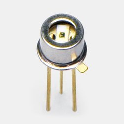
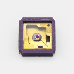
- Position sensors: Precisely measure the position of the wafer, photomask, and lens.
- Vibration sensors: Detect and compensate for vibrations that may affect alignment.
- Environmental sensors: Monitor temperature, humidity, and air quality, reducing the environmental impact on accuracy.
- Force and strain sensors: Ensure the force applied by actuators is accurate.
These sensors provide real-time data for closed-loop feedback systems, dynamically adjusting actuators to ensure precise patterning and accurate alignment. They can also detect deviations in real-time to prevent wafer defects and ensure perfect alignment of the photomask and wafer in multi-layer chip designs.
Centralized Control and Real-Time Data Processing
Sensors and actuators in lithography systems are connected through high-speed, low-latency communication protocols (such as EtherCAT or Ethernet) to ensure fast data exchange and coordination. A centralized control unit monitors and processes data from thousands of sensors and sends commands to actuators. This process relies on high-speed processors and complex algorithms to achieve nanometer-level precision.
As semiconductor node sizes continue to shrink, the integration of sensors and actuators becomes increasingly important. Interferometers measure the wafer stage position with nanometer precision, while actuators dynamically adjust the position based on sensor feedback. Optical sensors monitor light focus and intensity, and piezoelectric actuators adjust lenses or mirrors to maintain focus, ensuring the circuit design is accurately projected onto the wafer.
ADI’s Solution: ADAQ7768-1 µModule Data Acquisition System
ADI’s ADAQ7768-1 µModule data acquisition system integrates high-input impedance amplification, anti-aliasing filtering, signal conditioning, analog-to-digital conversion, and configurable digital filtering modules, providing high-performance signal chain solutions for lithography systems. The system ensures the stability and repeatability of the signal chain under temperature and power variations by integrating passive and active components.
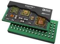
The 24-bit analog-to-digital converter (ADC) in the ADAQ7768-1 can precisely measure vibrations on the wafer stage, thermal variations of optical components, and sub-nanometer-level positional errors. Its compact design and ease of use make it an ideal choice for developing next-generation lithography equipment.
Conclusion
Advanced lithography systems rely on the synergy between thousands of sensors and actuators to achieve high precision and efficiency in semiconductor manufacturing. ADI’s ADAQ7768-1 data acquisition system, by integrating signal conditioning, conversion, and processing modules, simplifies the design of precision measurement and control systems, providing strong support for the future development of semiconductor manufacturing equipment. As semiconductor technology continues to advance, the role of sensors and actuators will become increasingly critical, driving ongoing innovation in smaller, more powerful, and energy-efficient chip technologies.