


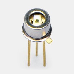
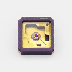


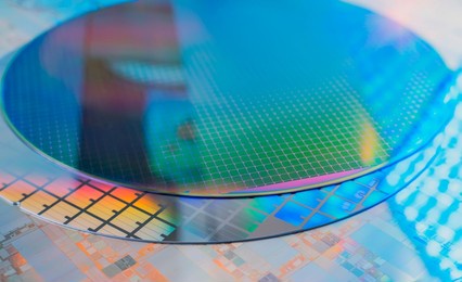
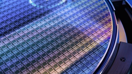
Semiconductor wafers are foundational components in the manufacturing of integrated circuits (ICs) and semiconductor devices. These wafers are thin, flat discs usually made from crystalline silicon, although other materials like gallium arsenide (GaAs) or silicon carbide (SiC) may be used for specific applications.
The wafers semiconductor manufacturing process is intricate and involves several key steps. It begins with the growth of a single crystal ingot, typically made of silicon. The ingot is then sliced into thin wafers through a process known as wafering. These wafers undergo meticulous processing steps, including polishing to achieve a smooth surface, doping to modify their electrical properties, photolithography for patterning, and deposition of various materials to create the necessary layers.
The size of semiconductor wafers is a critical factor, and common diameters include 4, 6, 8, and 12 inches. Larger wafers enable more chips to be produced in a single manufacturing batch, increasing efficiency and reducing costs.
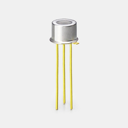
Once the processing is complete, the wafers are cut into individual chips, each containing integrated circuits. These chips are the heart of electronic devices, powering applications ranging from microprocessors and memory chips to sensors and other semiconductor-based technologies. The precise manufacturing of semiconductor wafers is essential to ensure the reliability, performance, and functionality of the resulting semiconductor devices.
Semiconductor wafers possess unique properties that make them crucial in electronics manufacturing. Typically made from crystalline silicon, these wafers exhibit semiconductor characteristics—intermediate electrical conductivity between conductors and insulators. The wafers have a high-purity, defect-free crystal structure, ensuring consistent electrical properties. They are flat, thin discs with precise thickness and diameter specifications. The surface is polished for uniformity, and the wafers can be doped to alter their conductivity. These properties make semiconductor wafers the foundational material for producing integrated circuits, microchips, and various electronic components essential in modern technology.

Semiconductor wafers play a pivotal role in the production of integrated circuits (ICs), serving as the substrate on which electronic components are fabricated. The process begins with the deposition of a thin layer of insulating material on the wafer’s surface. Next, a layer of semiconductor material, often silicon, is deposited and carefully patterned to create transistors, resistors, and other components.
Through a series of intricate steps involving photolithography and etching, the desired circuitry is etched onto the wafer. Dopants are then introduced to modify the electrical properties of specific regions, forming the transistors and other semiconductor devices. Multiple layers of these components are built up, interconnected by metal layers, creating a complex three-dimensional structure.
The entire wafer is then sliced into individual chips, each containing a complete set of interconnected electronic components. This precise and systematic process, known as semiconductor fabrication or semiconductor manufacturing, enables the mass production of ICs with incredible precision and miniaturization. The result is the creation of powerful and compact electronic devices that have become integral to our daily lives, from smartphones and computers to sophisticated control systems in various industries. If you are interested in our semiconductor wafers or any other electronic components, feel free to contact us!